Nanotechnology concept explained in simple examples
Nanotechnolgy is one of the most exciting subject nowadays. It is the magic behind the advancement of many gadgets we use in our day to day life. Our celphones, laptops, TVs, medicines, etc. they all use nanotechnolgy. The prefix nano is derived from the word nanometer, which is a length measurement. One nanometer is equal to ten to power minus nine meter (10-9 m). In another words, a human hair diameter/width is equal to 100 000 nm, which is very small. It is imposible to see it with a naked eye.
The question that an average person would ask is, what happen at such a tiny sizes? The answer is very simple and clear, the material properties changes at such a very small sizes. But wait a minute, how does that happen. Well, if you are smart enough to ask this question, that is what this blog post is all about, simple and intutive examples are provided to explain this magical phenomenon. Keep in mind that changing the size will change a material properties.
PRESENT Presenting soon? Rehearse with audience view • Get free metrics • Upgrade to advanced analysis & review Try it →Example 1
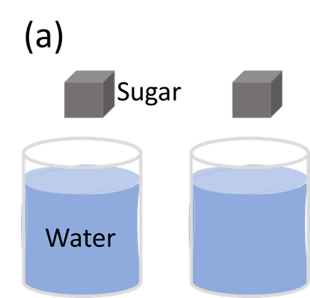
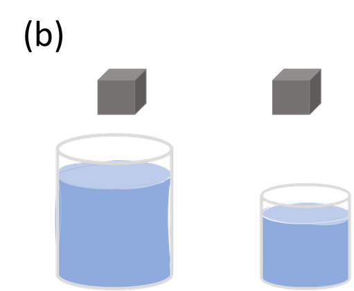
This example demonstrate the simplest explanation of nanotechnology phenomenon. Remember, shrinking the size of a material alters its properties. In this example, the material is sugar water and the property we want to change is the sweetness of that sugar water. Consider the scenario below in image (a), we have two cups of water, each cup contains the same amount of water, we added the same amout of sugar into each cup and mix them until all sugar in both cups is uniformly disolved. If we tested the sugar water on either of those cups, the level of sweetness will be the same, right? Yes. Lets consider the scenario in image (b), one cup size is being shrank and therefore the amount of water is less than the other cup, we added the same amount of sugar into each cup, and mixed them until the sugar is uniformly disolved. It is obvious that the level of sweetness of the small cup is higher (sweeter) than the big one. In this example, we succeeded to make our water sweeter without adding more sugar, but by only reducing the amout of water. Now, the intuition of nanotechnology phenomenon must start making sense to you.
Example 2
Surface to volume ratio is one of the key concepts in nanotechnology, it plays a huge role in improving a device
performance while maintaining its dimenssions. It is important to improve the efficiency of solar cells, light
emitting diodes, imaging contrast in medical imaging, TVs, to name a few. To understand surface to volume ratio concept,
lets look at the following scenario in the image below:
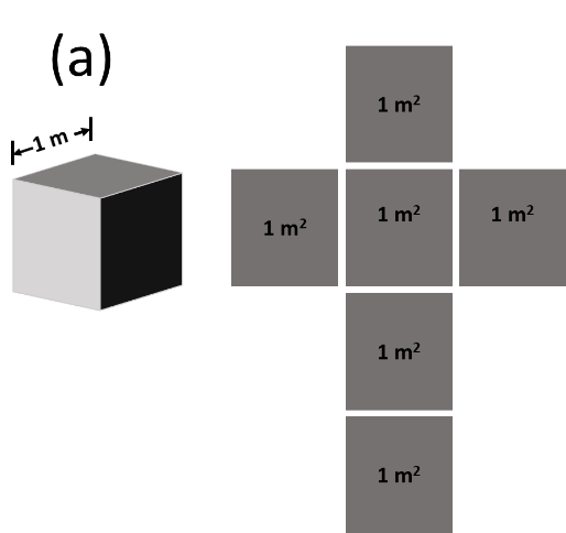
Consider a cube with 6 faces and 1 meter edge length [image (a)], the total volume of this cube is 1 m3, and the
surface area of each face is 1 m2. If we unfold the cube, the total surface area for the cube will be 6 m2. Lets
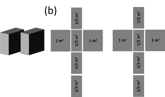
cut the cube into two halves and unfold each of them [image (b)]. The surface area of each half is 4 m2, which means
that the total surface area for both halves is 8 m2. The total volume of the two halves will remain the same as the
original cube in image (a) which is 1 m3. Just imagine we cut the cube into very tiny pieces, the surface area will
incearse dramatically while the volume remains unchanged.
Example 3
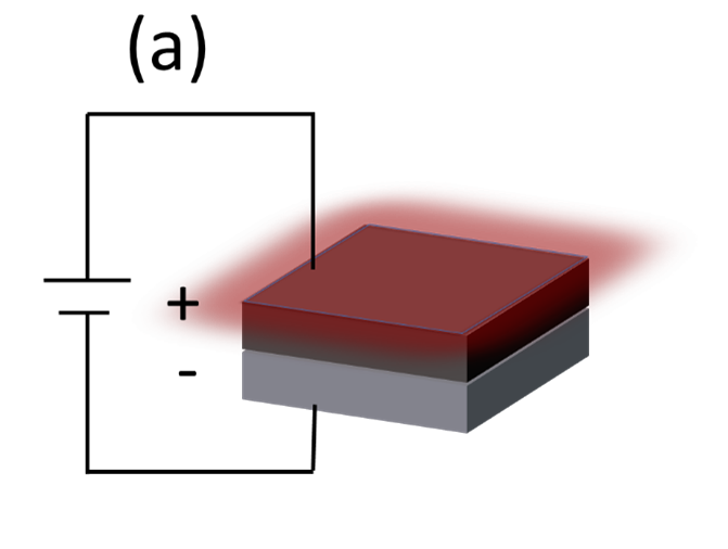
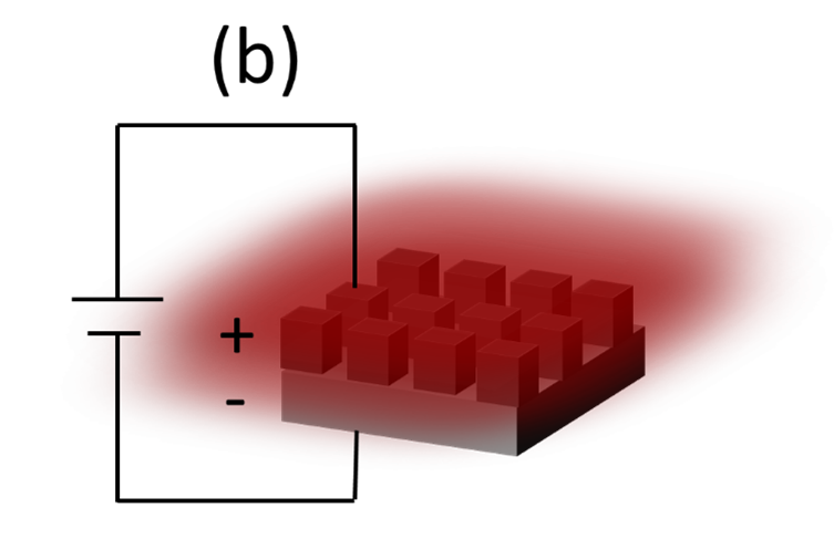
This example is abit technical, however, it is closley related to the previous example (2). The images bellow (a and b) are the simplest representations of light emitting diodes (LED). LED in its basic form is a junction consisting of two parts, n-type layer and p-type layer. When an LED is connected to a power supply, current will flow from the positive terminal of the power supply to the negative terminal, passing through the n-type and the p-type. Consequently, light is emitted from the top layer (emissive layer) of the LED. What is important to us is the surface area of the emissive layer (I guess you get the idea). The surface of the emissive layer of the LED in image (a) is flat, and therefore the amout of light emitted from the layer is restricted by the surface area of the emissive layer of the LED (a). Now it is time to pattern the emissive layer into smaller parts (image b), while maintaing the dimenssions of the LED. If you could still recall in example 2, you assume that the surface area is increased and as a result the light emitted will also increase, because the light is now emitted from a larger area than in image (a). In fact, this is one of the strategies that is used to enhance the effiency of solar cells.
Example 4
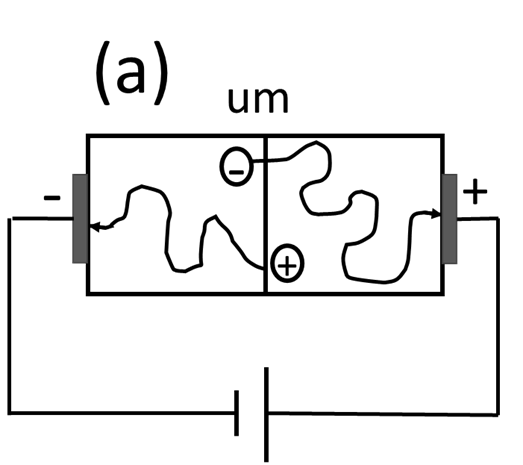
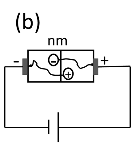
If you are some one who used old computers that were manufactured in early ninteath, and now using the comtemporarly computers, you may know the difference. Old computers are very slow, inefficient and freezes a lot specially if you are dealing with muliple tasks at the same time. The building block of any computer is transistors, and the size of the transistor matters in its performance and speed, how is matters that what this example will explain. A transistor consists of two diodes connected together, and therefore for simplicity we consider a diode as an example. A diode is made of n-type and p-type materials put toggether, when connected in a certain bias to an external power supply, negative charges travels from the n-type material to the positive terminal and vice versa for the positive charges. Consider the scenario in image (a) bellow where the diode size is about a few micrometers. For a charge to travel from one side to the opposite terminal, it may have to move around for long path before it reaches the terminal, and this process take some time (maybe in an order of microsecond or less). If we shrink the size of the diode to a few nanometers, the charge will travel less distance and therefore the time required to reach its destination (the opposite terminal) is less.
In conclusion
Nanotechnology is a very broad subject. It spans across different fields including physics, chemistry, biology, materials science, electronics, medicine, etc. There are many underlying phenomenon influencing a material or device properties. This blog post only addressed the basic concepts of nanotechnology. If you really interested to get into deeper understanding of it, you probably need a university degree in science, engineering or technology in at least one of the aforementioned fields.